
Replacing Global Wires with an On-Chip Network: A Power Analysis
Seongmoo Heo & Krste Asanovic
Introduction
Cross-chip global wires are becoming increasingly problematic as feature sizes shrink, with their delay and power consumption increasing rapidly relative to individual logic gates [1]. Long global wires also cause many design problems including routing congestion, noise coupling, and difficult timing closure. These worsening trends have led to proposals to replace design-specific global wiring with structured on-chip networks in large ASIC designs [2],[3]. Circuit blocks or tiles now communicate by sending packets across the on-chip network instead of driving signals across dedicated global circuit wires. The on-chip network links can be highly optimized by controlling their electrical environment to allow the use of optimized signaling techniques. Wiring efficiency can be improved by replacing a large number of low activity dedicated wires with fewer multiplexed communication links. Routers represent the main area and power overhead in an on-chip network.
We explore the power implications of replacing global wires with an on-chip network. We first develop detailed power models for power-optimized wires, including the effects of leakage current in a 70 nm process. We next examine the use of power-optimized wires in two contexts: 1) conventional ASIC or FPGA designs where dedicated global wires are replaced with dedicated but power-optimized wires, 2) tiled architectures, where all inter-tile global communication is via a dynamic packet-routed on-chip network using power-optimized links.
Wire Power Model
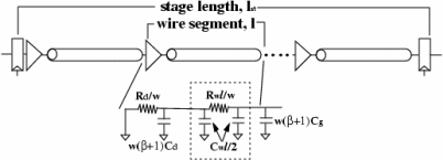
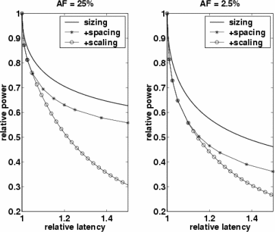
Figure 1 shows our first-order RC model of a long, pipelined and repeated wire. We can save power by using deeper pipelining to provide additional time slack in each wire stage. Although there are many ways of exploiting the time slacks obtained from pipelining, we focus on two variables: repeaters and supply voltage. We can either reduce the size and increase the spacing of repeaters, or scale down supply voltages, or both. Figure 2 shows latency-power curves of wires while varying repeater sizing, spacing, and supply voltage for different activity factors (AF).
|
|
On-Chip Interconnect Network Power Model
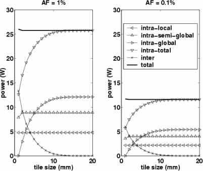
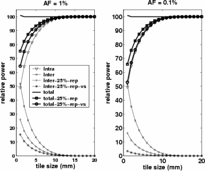
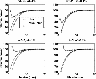
Wire-Routed Tiles: We now divide the chip into multiple tiles, and replace inter-tile wires with power-optimal pipelined wires. The number and total length of wires does not change. Figure 3 shows the wire power consumption of a tiled wire-routed design for varying the tile sizes. The wire power of the base chip is where the tile size is 20 mm (that is, when the whole chip is one tile). As the tile size decreases (smaller than half of the chip), intra-global wire power decreases exponentially while intra-semi-global or intra-local wire power remain roughly unchanged. However, the increase in power on inter-tile wires matches the power loss of the intra-global wires and so the total wire power stays roughly the same. Figure 5 shows the power saving of a tiled wire-routed chip when inter-tile latency is increased by 25 % and the network wires are pipelined. Smaller tiles result in greater power saving as more signals are pipelined. In particular, when leakage power is significant (AF = 0.1 %), pipelining through repeater optimization and voltage scaling is more effective at reducing the inter-tile wire power, since pipelining is more effective at saving leakage power
|
|
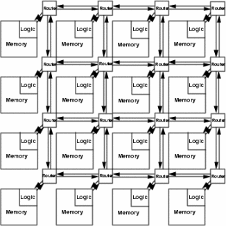
Packet-Routed Tiles: We finally consider a packet-routed tiled architecture. Figure 5 shows an example tiled ASIC architecture (4 by 4) and a mesh interconnect network. A mesh interconnect network was chosen since it is simple to design, power-efficient, and scalable. Tiles communicate with others only through routers and links between routers. On-chip network links are much cheaper in terms of area and power, than traditional off-chip network links. Thus it is natural that tiles exploit wider links than a single-tile chip does. However, an excessive number of on-chip IO wires result in a huge power and area overhead for routers. Usually, some degree of multiplexing and packet encoding are employed to reduce the number of IO wires while increasing the activity on link wires. We define the multiplexing factor, MF, as the ratio between activity on packet-routed link wires and that on the inter-tile wire-routed links they replace. Figure 6 shows the power consumption when considering the power overhead of routers while varying MF and AF.
|
|
Conclusion
Our results show that although power-optimized wires can reduce global wire power significantly (35-50%) in wire-routed ASIC or FPGA designs, it is difficult to achieve significant power savings in packet-routed tiled designs due to the energy expended in routers even for highly multiplexed inter-tile traffic. Tile sizes of around 2 mm on a side appear to provide the lowest total communication power in a 70 nm process.
Research Support
This work was partly funded by the NSF CAREER Award CCR-0093354, NSF ITR award CCR-0219545, and a donation from Intel Corporation.
References
[1] Ron Ho et al. The Future of Wires. In Proceedings of the IEEE, 89(4) , pp. 490-504, April 2001.
[2] M. Sgroi et al. Addressing the system-on-a-chip interconnect woes through communication-based design. In DAC, 2001.
[3] W. Dally and B. Towles. Route Packets, Not Wires: On-Chip Interconnection Networks. In DAC, pp. 681-689, 2001.
The Stata Center, Building 32 - 32 Vassar Street - Cambridge, MA 02139 - USA tel:+1-617-253-0073 - publications@csail.mit.edu (Note: On July 1, 2003, the AI Lab and LCS merged to form CSAIL.) |