
A Parameterizable FPGA Prototype of a Vector-Thread Processor
Jared Casper, Ronny Krashinsky, Chris Batten & Krste Asanovic
Introduction
We are developing a parameterizable FPGA prototype of the SCALE vector-thread processor [2]. The prototype has two main goals. First, to reduce the risk of the final custom chip implementation by allowing early rapid prototyping of many of the system interactions. Second, to provide a parameterizable prototype for architectural experiments.
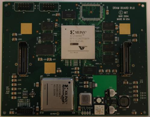
SCALE Prototype Board
The SCALE prototype board has been fabricated and consists of a single Xilinx XC2V4000 FPGA connected to a number of Micron DDR2 DRAMs that form the SCALE memory system. To support power measurements, the board is divided into multiple separate power islands. The board is attached to a test baseboard that provides sixteen independently measurable power supply connections and a byte-serial connection to a Linux PC that acts as the system host. Figure 1 is a picture of the board.
The current version of the board has a variety of additional DRAM parts with independent power supplies to support experiments in DRAM power control. The final version of the SCALE board will replace these additional DRAMs with a socket for the SCALE chip.
Risk Reduction
The original motivation for the development of the board was to reduce the risk in the full-custom SCALE chip design. The final SCALE board will use the Xilinx chip as a North Bridge , connecting SCALE to the DRAM memory system. SCALE has a high-bandwidth non-blocking cached vector memory system, with many complex interactions between multiple concurrent requestors and multiple outstanding memory requests [1]. The Xilinx chosen for the board is large enough to allow both the North Bridge memory controller and the SCALE processor and cache design to be prototyped together. The on-chip FPGA version of the processor can drive the memory system at approximately half the speed of the off-chip final SCALE chip, allowing a thorough debugging of memory system functionality.
Another advantage of the FPGA prototype is to provide a fast emulation system for SCALE software development, including compiler and applications.
Parameterizable Prototype
The full custom SCALE implementation will allow accurate characterization of area and power consumption for the vector-thread architecture, which is not possible with the FPGA prototype. However, the FPGA prototype supports rapid full system simulation of a large variety of vector-thread designs. Combining data from both prototypes will allow both accurate and extensive characterization of the space of possible vector-thread designs.
In particular, we are interested in the design of the memory subsystem, which is the most critical component in terms of overall system performance and power consumption. We intend to use the FPGA prototype board to investigate various power/performance tradeoffs, including the effects of varying cache parameters and replacement policies, prefetch strategies, DRAM access scheduling policies, use of DRAM powerdown modes, and of different DRAM types (e.g., DDR2 versus Mobile DRAM).
Status
A single-issue seven-stage pipeline MIPS processor core has been completed and mapped to the board and passes our MIPS verification test suite. This core will form the SCALE control processor. The DDR2 memory controllers have been completed and tested in isolation using simple memory traffic generators. The next steps in development are the cache subsystem and the vector-thread unit.
Acknowledgements
This work was partly funded by an NSF CAREER Award CCR-0093354, DARPA PAC/C Award F30602-00-2-0562, an NSF Graduate Student Fellowship, the Cambridge-MIT Institute, Infineon, SGI, and equipment donations from Xilinx and Intel.
References:
[1] C. Batten, R. Krashinsky, S. Gerding, and K. Asanovic. Cache refill/access decoupling for vector machines. In MICRO-37, 2004.
[2] R. Krashinsky, C. Batten, S. Gerding, M. Hampton, B. Pharris, J. Casper, and K. Asanovic. The vector-thread architecture. In ISCA-31, 2004.
The Stata Center, Building 32 - 32 Vassar Street - Cambridge, MA 02139 - USA tel:+1-617-253-0073 - publications@csail.mit.edu (Note: On July 1, 2003, the AI Lab and LCS merged to form CSAIL.) |