
VIsolate: Voronoi Toolpaths for PCB Mechanical Etch
Marsette A. Vona & Daniela Rus
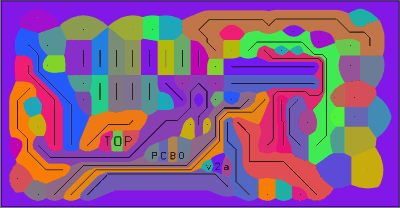
The Voronoi regions (colored areas) corresponding to the traces (along
the black lines) of a PCB.
PCB Mechanical Etch
Printed Circuit Boards (PCBs) are in virtually every piece of modern electronics. They usually start out as a sheet of fiberglass or phenolic coated on one or both sides with a continuous sheet of copper (called cladding). In normal manufacturing, a photochemical process removes much of that copper, leaving a pattern of traces (i.e. wires) to which electronic components are soldered to form the desired circuit.
For some applications, particularly very low-volume production, production in home or office environments, and rapid-design cycle R&D environments, the setup costs, environmental hazards, mess, and, not least, sensitivity of such photochemical processes to many variables, suggest that other methods of PCB production be explored.
Mechanical etch is one major alternate method for PCB production. This process also starts with a copper-clad board. However, the unwanted copper is removed mechanically rather than chemically. Most often, a fine-point rotary tool bit is used to create a separation in the copper around the boundary of each trace (like the middle board in the picture below). The extra copper remaining between the traces is usually left in-place, as it is no longer electrically connected to any trace.
There are a number of commercial systems already available which perform mechanical etch by cutting such trace outlines, for example LPKF's products. We were are interested in an alternate method: compute the Voronoi region associated with each trace and cut along the boundaries between such regions. This method may have some advantages, as we describe next.
Voronoi Toolpaths
The standard practice of cutting a loop around the boundary of each trace will always produce two cutter passes between any two adjacent traces, even when the traces are so closely spaced that these passes may overlap. This results in an unnecessarily long toolpath, which translates to longer production time. Even when the passes do not quite overlap, we must still consider second-order effects which may degrade the geometry of such closely spaced cuts, e.g. play in the machine and flexing of the cutter (effects which may be exacerbated in the lowest-cost hardware). By merging the two passes into one in such cases, we can get a single pass maximally distant from both traces. In many cases that would also effectively widen the traces, thus increasing current carrying capacity, which is a concern in tiny circuits that must carry power. This motivation led us to the concept of Voronoi toolpaths: we compute a generalized Voronoi diagram using the PCB traces as Voronoi sites, and then we cut only along the boundaries between the resulting Voronoi regions [1].
VIsolate
We have implemented a prototype software system called VIsolate (Voronoi Isolate) which computes both standard outline toolpaths and our novel Voronoi toolpaths using an adaptation of the graphics-hardware-based generalized Voronoi diagram algorithm described by Hoff et al in [2] and on the raster-to-vector algorithms employed in Selinger's Potrace program [3]. We have tested VIsolate by cutting several PCBs on a Sherline CNC mini-mill. Two of these PCBs are shown below (middle, right).
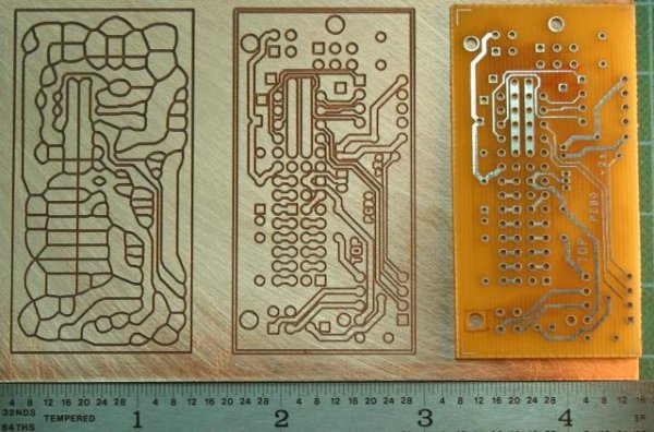
The same printed circuit board manufactured three different ways: by traditional
photochemical process (right); by mechanical etch with standard outline
toolpaths (middle); by mechanical etch with Voronoi toolpaths (left).
The board on the right has also had additional processing: it has been
drilled and tin-plated.
References:
[1] Marsette A. Vona, and Daniela Rus. Voronoi toolpaths for PCB mechanical etch: Simple and intuitive algorithms with the 3D GPU. In Proceedings of the International Conference on Robotics and Automation, 2005.
[2] K. E. Hoff, III, J. Keyser, M. Lin, D. Manocha, and T. Culver. Fast computation of generalized Voronoi diagrams using graphics hardware. In Proceedings of the 26th annual conference on Computer graphics and interactive techniques, ACM Press/Addison-Wesley Publishing Co., pp. 277--286, 1996.
[3] P. Selinger. Potrace: a polygon-based tracing algorithm. Unpublished, available at http://potrace.sourceforge.net/potrace.pdf, September 2003.
The Stata Center, Building 32 - 32 Vassar Street - Cambridge, MA 02139 - USA tel:+1-617-253-0073 - publications@csail.mit.edu (Note: On July 1, 2003, the AI Lab and LCS merged to form CSAIL.) |